
Products
Featured products
 Diffractometer1. The accuracy of Diffractometer is high. 2. The application range of Diffractometer is wide. 3. Diffractometer is easy to operate, convenient and efficient.More
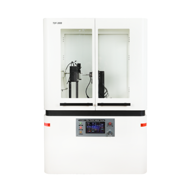
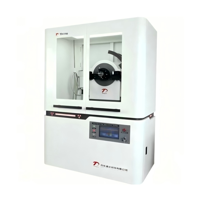
- Single Crystal XRD1.The single crystal machine adopts PLC control technology. 2.Modular design, accessories plug and play. 3.Electronic lead door interlocking equipment with double protection. 4.Single crystal X-ray tube: a variety of targets can be selected, such as Cu, Mo,etc. 5. Single crystal adopts four-circle concentric technology to ensure that the center of no goniometer remains unchanged.More
- Series X-ray Crystal Analyzer1. X-ray instrument is easy to operate and fast to detect. 2. X-ray instrument is accurate and reliable, with excellent performance. 3. X-ray instrument has various functional accessories to meet the needs of different testing purposes.More
- Powder Diffractometer1. Detector type: Array detector or SDD detector; 2. PLC automatic control calculus, Integration mode conversion, PLC automatically performs PHA, dead time correction 3.Sample measurement type: powder sample, liquid samples, melt-state samples, viscous samples, loose powders, bulk solid samples 4.Available with a variety of diffractometer accessories 5.Maximum output powder: 3kWMore

Contact us


Thin Film Diffraction
- Tongda
- Liaoning, China
- 1—2 months
- 100 units per year
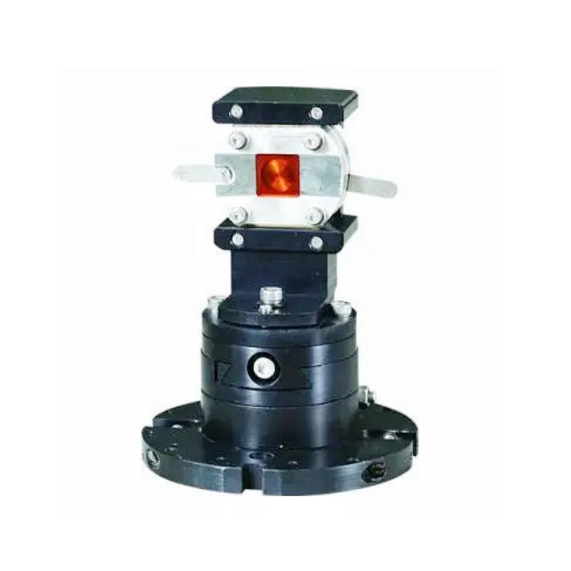
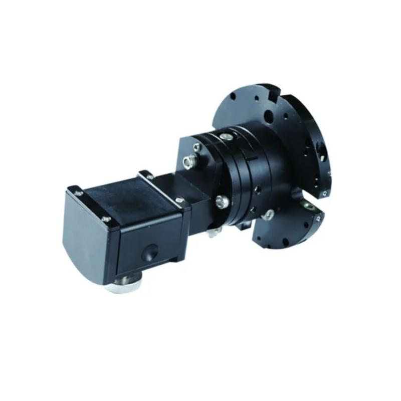
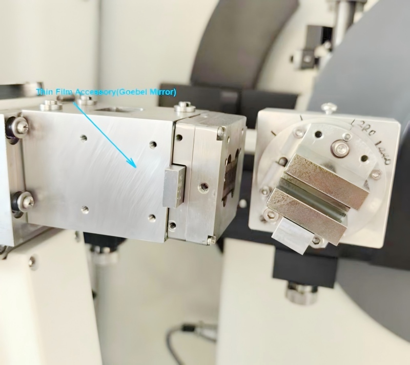
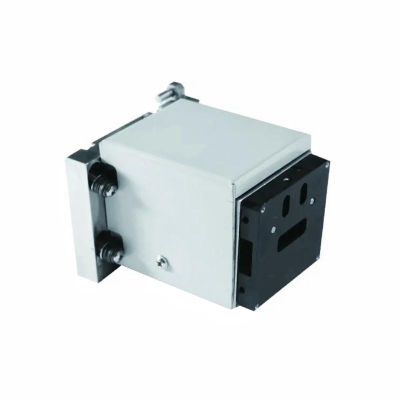
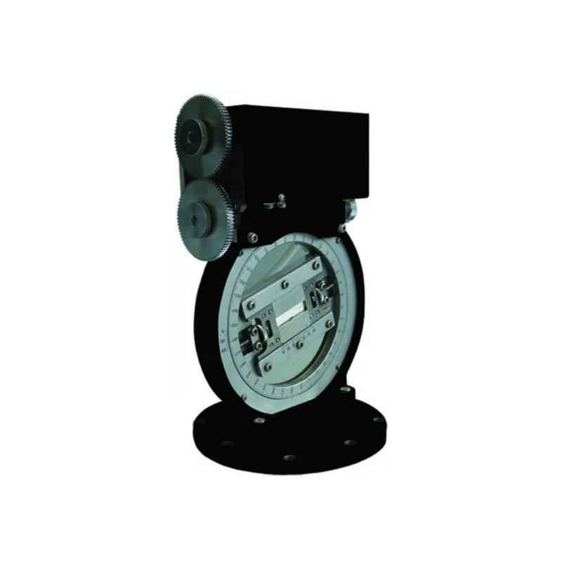
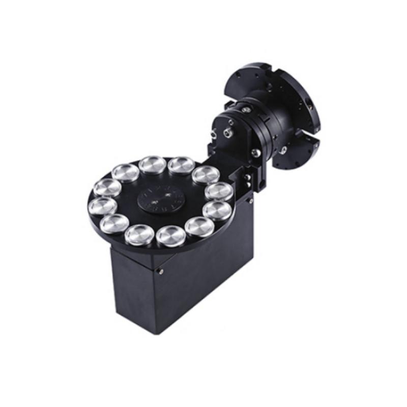
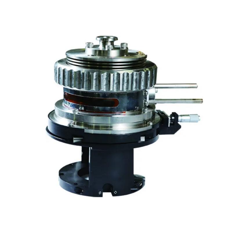
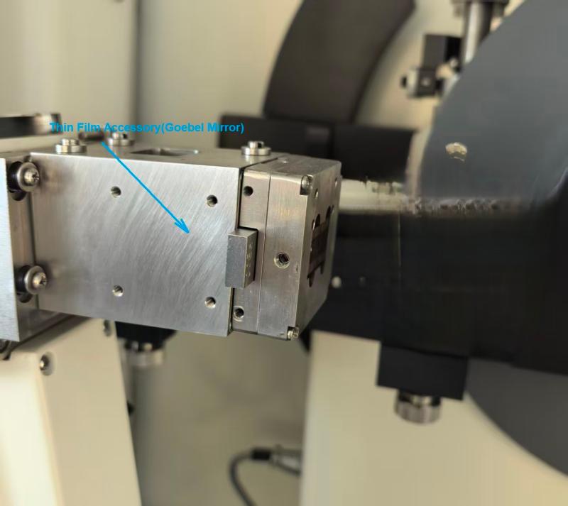
Introduction to Thin Film Attachment
X-ray testing techniques are widely employed in the characterization of various thin film materials. Thin film materials differ from conventional powder XRD analysis due to their structural particularities and limitations. For instance, when a thin film exhibits strong preferred orientation, only diffraction signals from specific crystal planes can be observed, making characterization significantly more challenging compared to powder samples. The thin film attachment enhances characterization accuracy by incorporating longer collimator slits to effectively filter scattered radiation, reduce substrate interference, and intensify the diffraction signal from the thin film itself. Specifically designed to address low signal intensity and high background noise in thin film materials, this attachment is suitable for analyzing samples with thicknesses ranging from nanometers to micrometers.

Applications of Thin Film Attachment
The thin film attachment serves as a standard tool for semiconductor material characterization and is extensively used in R&D and quality control across materials science, nanotechnology, and semiconductor materials and devices. It is suitable for testing various thin film samples, particularly for structural analysis of epitaxial thin films and single crystal wafers, enabling phase identification, orientation degree analysis, and stress testing. Specific applications include:Metallic and Ceramic Materials: Evaluating the texture of rolled sheets, ceramic orientation, and residual stress (e.g., wear resistance and machinability analysis).
Multilayer and Functional Films: Analyzing coating structures such as magnetic films, surface-hardened metal layers, and high-temperature superconducting films, as well as interface characteristics of multilayer films on glass, silicon wafers, and metal substrates.
Polymer and Special Materials: Investigating orientation and stress in macromolecular materials like paper coatings and optical lens films.

Advantages of Thin Film Attachment
High-Efficiency Data Acquisition: Supports high-speed scanning and rapid data processing, enhancing testing efficiency and suitability for high-throughput experimental environments.
User-Friendly Operation and Stability: The attachment’s structural design simplifies calibration procedures, enabling quick sample positioning and testing. Its core components are optimized for extended service life and compatibility with mainstream equipment such as the TD series X-ray diffractometers.
Powerful and Intelligent Functionality: Integrates multiple measurement modes (e.g., transmission/reflection pole figure testing, stress analysis) and enables automated control and data analysis via software, significantly improving detection accuracy and operational intelligence.
Through technological innovation, the thin film attachment addresses key challenges in thin film material characterization and delivers a reliable solution for advanced material R&D and quality control.

Why Choose Tongda
As a contractor for the National Major Scientific Instruments and Equipment Development Special Project sponsored by China's Ministry of Science and Technology, Tongda leads a collaborative effort involving seven prestigious institutions including Sun Yat-sen University and the Shenyang Institute of Computing Technology, CAS. In 2013, we established an Academician Workstation in partnership with Academician Chen Xiaoming. After eight years of dedicated R&D, we achieved a historic milestone in 2021 by launching China's first domestically developed X-ray single crystal diffractometer with fully independent intellectual property rights—marking a breakthrough from "0 to 1" in this field.

With R&D personnel comprising 30% of our workforce—significantly above industry average—we have accumulated 23 patents and 7 software copyrights. Our comprehensive product portfolio includes the TD Series Diffractometers, Benchtop Diffractometers, X-ray Fluorescence Spectrometers, X-ray Single Crystal Diffractometers, Crystal Orientation Instruments, and Crystal Analyzers.
Our Tongda AI Automatic Diffractometer represents an industry-leading integration of precision robotic manipulation with artificial intelligence: It supports autonomous sample handling for powders, thin films, and bulk materials; enables remote control via mobile APP with automatic door opening/closing for enhanced operational safety; features modular design for easy upgrades and maintenance with powerful expandability.

When you choose Dandong Tongda Science & Technology Co., Ltd., you receive more than precision instruments—you gain: continuous technical support from our Academician-led expert team, rapid response capabilities backed by our 30% R&D workforce, system integration expertise accumulated through national-level major projects, and proven reliability trusted by multiple prestigious institutions.