


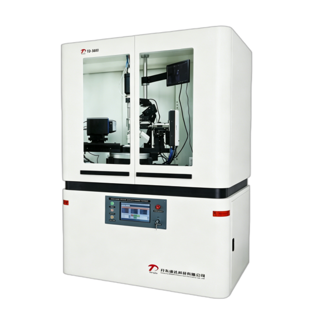
X-ray testing is a non-destructive testing method that does not damage the object itself, and has been widely used in material testing (QC), failure analysis (FA), quality control (QC), quality assurance and reliability (QA/QC), research and development (R&D) and other fields.
It can be used to detect defects (cracks, delamination, voids, etc.), such as delamination and cracks in electronic components, light-emitting diodes, metal substrates, etc., and by detecting image contrast to determine whether there are defects in material, shape, size, orientation, etc.

In the semiconductor industry, X-ray inspection equipment is commonly used to detect the quality of chips and wafers, as well as possible defects in the manufacturing process. It is mainly reflected in the following aspects:
1. Defect detection in the wafer production process: there may be problems such as gas, defects, foreign bodies in the wafer production process, and X-ray inspection equipment can scan the wafer and detect these problems to ensure production efficiency and wafer quality.
2. Packaged finished product inspection: Packaged finished product is the next step after the completion of wafer production. X-ray inspection can scan the finished product and play an important role in detecting the shape of the finished product and the quality of the solder joint to ensure the integrity and quality of the finished product.
3. Chip defect detection: there may be defects in the chip manufacturing process, including dead pixels, defective circuits, etc. These defects can cause the chip to not work properly, so X-ray inspection equipment is needed to detect defects in the chip and find and resolve the problem in a timely manner.
The faster the sample validation during semiconductor packaging and testing, the more likely it is that its products will be brought to market quickly. The business model of seamless docking of chip design companies and semiconductor packaging and testing plants for mass production, outsourcing mass production to large packaging factories after product quality and yield are fully verified, and the seamless docking of mass production helps chip companies do not have to worry about the packaging process and promote new models in the field of packaging and testing.
As a link in the semiconductor packaging and testing industry chain, X-ray non-destructive testing technology has realized 100% online testing in the field of semiconductor packaging and testing, and has become a necessary means to verify product quality. With the iterative updating of new semiconductor chip technology, non-destructive testing is facing more and more pressure. First, the requirements for detection efficiency are getting higher and higher. Secondly, the difficulty of detection has also increased, the previous packaging technology can also see the pin with the naked eye, and now the BGA technology can not see most of the welding ball, only X-ray fluoroscopy detection.
The semiconductor industry is far ahead of other industries, has the fastest capacity and technology iterations, and has now long been an invisible production mode, the size of the fingernail coverage area can carry tens of billions of transistors. The chip will be put on the market before a series of precise and complex validation processes, as chip sizes are designed to become smaller and smaller, X-ray inspection equipment with high magnification and resolution is required, and inspection accuracy is required to ensure that important welding defects are not missed.
To this end, X-ray inspection technology is also constantly upgrading technology, developing in the direction of high precision and intelligence, and keeping up with the new trends and new requirements of semiconductor packaging and testing to meet the testing requirements of semiconductor chips.


In addition, X-ray inspection equipment can be used to inspect packaged automotive-grade power semiconductors to help improve product consistency. Using the penetration of X-rays, it is possible to conduct a 100% comprehensive online inspection of high-capacity power semiconductors without damaging the appearance of the product, ensuring that all automotive semiconductors delivered by the factory are free from defects during the production process and improving product reliability.