Crystal Orientation Instrument: The Navigator for Semiconductor & Optical Material Processing
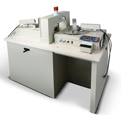
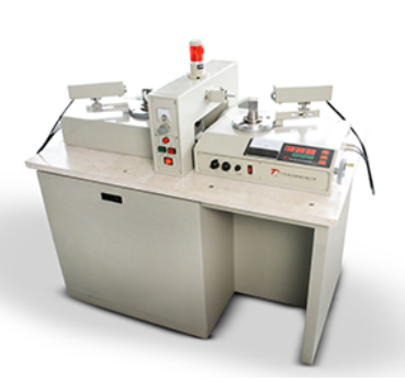
2026-02-09 08:46In high-end manufacturing fields such as semiconductor chips and optical components, the crystal orientation accuracy of materials directly determines product performance and service life. As a core inspection equipment before processing, the crystal orientation instrument acts as a precise "crystal orientation navigator." It accurately identifies the internal atomic arrangement direction of crystals, providing precise guidance for subsequent processing steps such as cutting, grinding, and polishing. This instrument is a critical prerequisite for ensuring the quality of high-end material processing and is widely used in high-tech industries such as semiconductors, optics, aerospace, and aviation.

The core role of the crystal orientation instrumentis to address the challenge of the "invisible internal crystal orientation" of crystalline materials, enabling precise positioning and quantitative detection of crystal orientation. The physical, chemical, and optical properties of crystalline materials are anisotropic, meaning that hardness, toughness, refractive index, and other characteristics vary significantly across different crystal orientations. For example, semiconductor silicon wafers exhibit notable differences in conductivity and etching rates depending on their crystal orientation. If the orientation deviates during processing, it can lead to chip leakage, unstable performance, or even complete failure. Leveraging core technologies such as X-ray diffraction, laser interferometry, or electron backscatter diffraction, the crystal orientation instrument can quickly capture diffraction signals from the internal atoms of crystals without causing damage. Through data analysis, it accurately calibrates crystal orientation angles with errors ranging from a few seconds to a few arcminutes, providing an accurate angular reference for processing steps.
As a "navigation device" before processing, this orientation instrument offers the core advantages of speed, precision, and non-destructiveness, making it ideal for high-end material processing requirements. Traditional crystal orientation methods relied on manual experience, which was not only inefficient but also prone to significant errors, failing to meet the high-precision demands of semiconductor and optical material processing. In contrast, modern crystal orientation instruments employ intelligent detection technology, completing a single measurement in just seconds to minutes. They enable automated identification, calibration, and data recording of crystal orientations, significantly improving inspection efficiency. Moreover, their detection accuracy meets the highest industry standards and is compatible with various crystalline materials, including silicon, germanium, sapphire, quartz, and diamond. Whether dealing with bulk raw materials, thin slices, or tiny crystals, precise orientation can be achieved through non-destructive testing, avoiding material loss.
In the semiconductor industry, the crystal orientation instrument serves as the "first quality checkpoint" in chip manufacturing. Semiconductor chips rely on crystalline substrates such as silicon or silicon carbide wafers. Before processing, these substrates must be accurately calibrated for crystal orientation using the orientation instrument to determine the cutting direction and angle. This ensures that the arrangement of transistors and the direction of current transmission align with design requirements during subsequent photolithography and etching processes. For example, in photovoltaic-grade silicon wafer processing, the orientation instrument can precisely locate key crystal orientations such as (100) and (111), guiding cutting equipment to slice along optimal orientations to enhance the photoelectric conversion efficiency of the wafers. In silicon carbide chip manufacturing, precise orientation helps reduce chipping and cracks during cutting, lowering chip failure rates and supporting the large-scale production of high-end semiconductor devices.

In the field of optical material processing, the crystal orientation instrument plays an equally essential role as a navigator. Optical components such as lenses, prisms, and laser crystals require high consistency in crystal orientation. Deviations in orientation can lead to abnormalities in light refraction and reflection, affecting the imaging quality of optical systems and laser output efficiency. This instrument can accurately detect the optical axis direction of optical crystals, guiding processing equipment to perform grinding and polishing along the optical axis. This ensures that the light transmittance and refractive index of optical components meet design standards, making it widely applicable in the manufacturing of products such as camera lenses, laser devices, and optical instruments.
Furthermore, the intelligent upgrades of crystal orientation instruments have further enhanced their "navigation" value. Modern crystal orientation instruments can interface with computers and cutting equipment, transmitting detected orientation data in real time to processing systems. This enables automatic adjustment of cutting angles and paths, achieving an integrated "detection-processing" workflow. This significantly reduces human operational errors while improving processing efficiency and product consistency. Additionally, these devices are equipped with data storage and traceability functions, allowing the recording of orientation data for each batch of crystals. This facilitates quality control and subsequent issue analysis, making them suitable for large-scale industrial production needs.
As the "crystal orientation navigator" for semiconductor and optical material processing, the crystal orientation instrument addresses the challenge of crystal orientation positioning with its precise, rapid, and non-destructive detection capabilities. It provides reliable support for subsequent processing steps, directly influencing the performance and quality of high-end products. As the semiconductor and optical industries advance toward higher precision and miniaturization, this instrument will continue to evolve and upgrade, solidifying its role as a core inspection device driving the high-quality development of high-tech industries.

